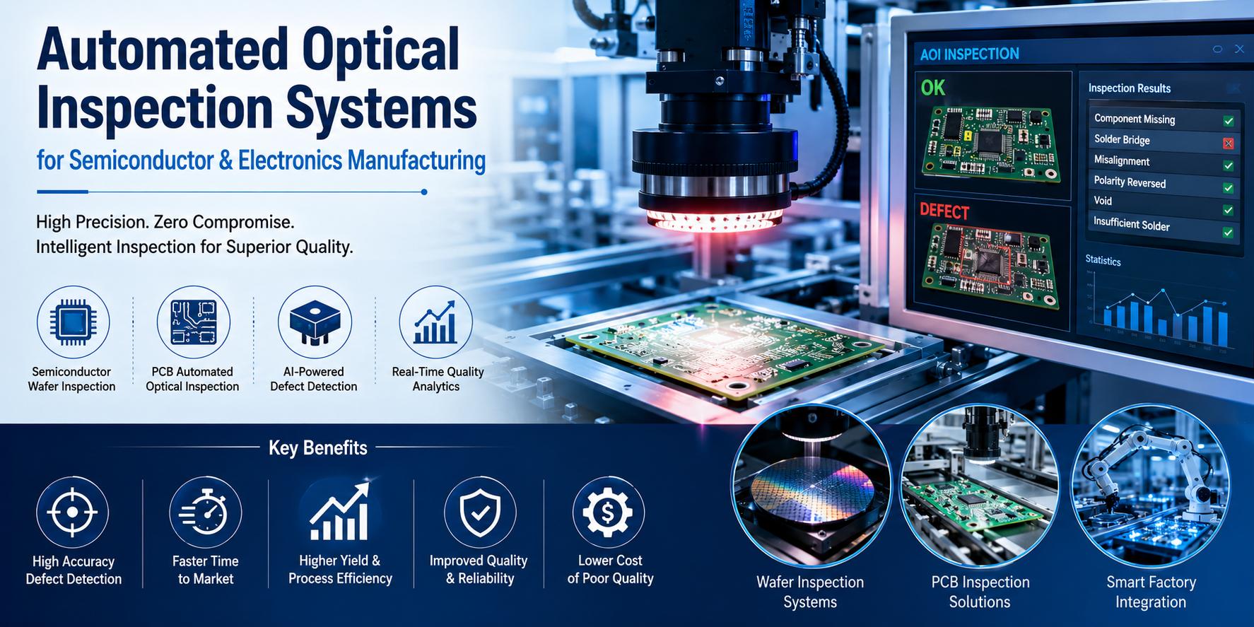
Automated Optical Inspection Systems For Semiconductor & Electronics Manufacturing
Introduction
As semiconductor devices become smaller, more complex, and more performance-driven, maintaining manufacturing quality has become increasingly challenging. Even microscopic defects can impact device functionality, reduce yield, and increase production costs. To address these challenges, manufacturers rely on Automated Optical Inspection Systems to detect defects quickly and accurately throughout the production process.
Modern AOI Systems have become a critical component of semiconductor and electronics manufacturing, enabling real-time defect detection, process monitoring, and quality assurance. From wafer fabrication to PCB assembly, these systems help manufacturers maintain high standards while supporting Industry 4.0 initiatives and smart factory operations.
This article explores how AOI for Semiconductor Manufacturing improves quality control, enhances yield, and supports advanced manufacturing environments.
What Are Automated Optical Inspection Systems?
Automated Optical Inspection Systems are advanced machine vision platforms that use cameras, optics, lighting technologies, and intelligent software algorithms to inspect products for defects without human intervention.
Unlike manual inspections, which can be time-consuming and prone to inconsistency, AOI technology performs rapid and repeatable inspections across large production volumes.
These systems are commonly used for:
- Wafer inspection
- PCB assembly verification
- Surface defect detection
- Packaging inspection
- Component placement validation
- Final product quality verification
By implementing AOI Systems, manufacturers can identify process issues early, reduce scrap rates, and improve overall production efficiency.
The Growing Importance of AOI in Semiconductor Manufacturing
Semiconductor manufacturing involves hundreds of highly controlled process steps, including lithography, etching, deposition, and packaging. A single defect introduced during any stage can impact device performance.
This is where AOI for Semiconductor Manufacturing plays a vital role. Inspection systems continuously monitor production quality and provide actionable data for process engineers.
Key benefits include:
Enhanced Semiconductor Manufacturing Quality Control
Manufacturers must maintain extremely tight tolerances to meet industry specifications. Advanced inspection platforms strengthen Semiconductor Manufacturing Quality Control by identifying defects before they reach downstream processes.
Improved Yield Performance
Yield loss can significantly affect profitability. By detecting abnormalities early, inspection systems help engineers correct process deviations before they impact large batches of products.
Faster Root Cause Analysis
Modern AOI platforms generate detailed inspection reports that allow engineering teams to trace defect sources and implement corrective actions quickly.
Applications Across Semiconductor Production
Wafer Inspection Systems
During wafer fabrication, particles, scratches, pattern defects, and contamination can compromise device performance. Advanced Wafer Inspection Systems use high-resolution imaging and sophisticated algorithms to identify these issues at an early stage.
These inspections help fabs:
- Reduce yield loss
- Improve process consistency
- Increase production reliability
- Support advanced node manufacturing
As technology nodes continue to shrink, wafer-level inspection becomes increasingly important for maintaining competitive manufacturing performance.
Semiconductor Defect Detection
One of the primary objectives of inspection technology is effective Semiconductor Defect Detection.
Common defects identified include:
- Pattern irregularities
- Surface contamination
- Cracks and scratches
- Alignment errors
- Missing structures
- Process-induced anomalies
Modern AOI Systems can classify defects automatically, helping engineers prioritize corrective actions and improve manufacturing efficiency.
PCB Automated Optical Inspection in Electronics Manufacturing
Beyond semiconductor fabs, inspection technology is widely used in electronics assembly operations.
PCB Automated Optical Inspection solutions verify component placement, solder joint quality, polarity orientation, and assembly accuracy. These inspections reduce product failures and improve customer satisfaction.
Typical inspection checkpoints include:
- Solder paste inspection
- Component placement verification
- Missing component detection
- Solder bridge identification
- Lead alignment verification
For electronics manufacturers operating high-volume production lines, Automated Optical Inspection Systems provide an effective method of maintaining consistent product quality while minimizing manual labor requirements.
AI-Based Optical Inspection and Industry 4.0
Recent advances in artificial intelligence are transforming inspection capabilities across semiconductor manufacturing facilities.
Traditional rule-based inspection systems often struggle with complex defect patterns and process variations. Modern AI-Based Optical Inspection platforms leverage machine learning algorithms to improve detection accuracy and reduce false alarms.
Benefits of AI-driven inspection include:
- Adaptive defect recognition
- Continuous learning capabilities
- Faster classification of anomalies
- Improved process optimization
- Reduced operator intervention
By integrating AI with AOI for Semiconductor Manufacturing, organizations can achieve higher inspection accuracy and more proactive quality management.
Machine Vision Inspection Systems for Smart Factories
The rise of Industry 4.0 has accelerated the adoption of intelligent inspection technologies.
Today's Machine Vision Inspection Systems are integrated with manufacturing execution systems (MES), factory automation platforms, and analytics tools. This connectivity enables real-time production monitoring and data-driven decision-making.
Smart inspection platforms can provide:
- Automated alerts
- Process trend analysis
- Statistical process control
- Yield optimization insights
- Predictive quality monitoring
These capabilities transform inspection from a reactive quality-control function into a strategic manufacturing intelligence tool.
Automated Visual Inspection and Future Manufacturing Trends
The future of manufacturing quality control is increasingly dependent on Automated Visual Inspection technologies.
Emerging trends include:
3D Inspection Technology
Three-dimensional imaging enables more accurate measurement of complex structures and package geometries.
AI-Powered Defect Analytics
Advanced analytics platforms can predict quality issues before they occur, reducing production disruptions.
Real-Time Factory Integration
Inspection systems are becoming tightly connected with factory automation solutions, enabling immediate corrective actions.
Edge Computing and Cloud Analytics
Manufacturers can analyze inspection data across multiple production facilities, improving global operational consistency.
As semiconductor complexity continues to increase, AOI Systems will remain essential for maintaining quality, yield, and operational excellence.